Keyboard Shortcuts
Likes
Search
LN 1530 Wellbrook amplifier replica deaf on LW - MW
|
Good morning, I'm wondering if anyone like me has made a full working Wellbrook 1530 LN amplifier based on the schematic found in the files section named "Wellbrook_Loops.Kicad_sch." with smd 2SK932 jfets (but others schematics are very similar) I'm asking because I made a couple of them over time, one even with the original 2SK715 jfets but in the end they have the same problem, that is, they seem completely deaf up on LW and MW to the shortwave range, where they work much better...a classic amplifier with only two transistors (BFU590QX) works regularly. I tested the jfets (taken from the European electronics e-commerce portal TME) and they are all ok, the absorption is normal at about 115 mA at 12V. The toroid windings are the ones described on the schematic: input P3/S12 (plus the two single turns) secondary with crossed wires - output P9/S5. Test loop hang from a tree in my garden at about 2 mt. from ground.? I'm adding the link with a short video and I've put two photos of the boards so you can see the construction. Thanks in advance, F.
?
?
? |
|
I think you may have a oscillation problem that is causing your problem on the lower frequencies. You need to make the board more compact and you need double sided copper shielding on the board.
?
I have designed several PCBs for the ALA1530LN and they all work fine, with no oscillation issues.
?
Everett N4CY
In a message dated 1/2/2025 12:55:57 PM Central Standard Time, netsmo62@... writes: ?
|
|
Martin,
?
His ALA1530LN clone is working on 7 MHz without any problem, but in not working on 2MHz and below.
?
Everett
In a message dated 1/2/2025 1:28:50 PM Central Standard Time, martin_ehrenfried@... writes: ?
|
|
Yes, I understand that, but if it is close to oscillation, due to incorrect transformer phase, the gain can appear to be much higher at mid-frequencies.
?
I have seen this myself with some builds.
?
Regards,
?
Martin
?
?
On Thu, Jan 2, 2025 at 07:46 PM, Everett N4CY wrote:
His ALA1530LN clone is working on 7 MHz without any problem, but in not working on 2MHz and below. |
|
I can't see anything called "Wellbrook_Loops.Kicad_sch" in the files section, can you provide a link ?
?
Regards,
?
Martin
?
On Thu, Jan 2, 2025 at 06:55 PM, Francesco Caizzi wrote:
the schematic found in the files section named "Wellbrook_Loops.Kicad_sch." |
|
I have built several from the esign in:
?
?
So far two of he 1530 configuration and one of the 100 configuration have been built and tested. The PCB is designed to fit into a Hammond 1555E2GY enclosure. It is two sided with ground fills on both sides.
?
Since it is winter here I have not tested them outside but have done preliminary 3/4MHz IMD tests.
--
=================================================================== Mike M |
开云体育Hi Francesco, Have you used a nanovna to sweep the gain and input impedance? You'll need a 1:1 input transformer (unbalanced to balanced). You'll also need an attenuator on? the nanovna TX output to reduce the level, I'd suggest something like 20 dB so the loop amp isn't being overloaded. If you sweep it please post the results. 73, Steve AA7U On 1/2/2025 11:55 AM, Francesco Caizzi
via groups.io wrote:
|
|
Good morning, sorry if I didn't answer all the appreciated replies but yesterday I sat there to do some tests and I have to say that maybe the apparent poor sensitivity on the low ranges of the LN amplifier can also be attributed to the positioning of the loop? In fact I moved the test loop (1 mt) inside the laboratory connected to the T-Bias with another shorter test cable (even if the longer external cable is fine) and things seem to be going better. It is true that maybe positioning the loop on a branch of a tree (about two meters high) with a metal net less than three meters away plus one of those mobile shelters for cars probably also made of metal structure, with a sheet metal shed on the side also less than three meters away... maybe it's not the best condition for this reception band, while on others with other types of propagation it goes decidedly better. I tried with the sample made both with the two types of jfet (2SK932 and original 2SK715) and with the normal two transistors amplifier with the BFU590 (qx) and the results are more or less similar, so... I don't think there are problems of construction or electronic components. Having said that, I answer individually to those who answered me:
?
Dave Martin: What do you mean? The coupling capacitors are those in the diagram, already used similarly in other amplifiers.
?
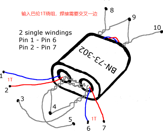
Tom VE3PSZ: Ferrite material is always 73. BN 73-302 ferrite core.
?
Steve Ratzlaff: Yes, I have had a NanoVNA from some time and in fact I really needed to understand how to do some bench tests of the amplifiers with that instrument. I made a diagram that I put together with the photos of the two boards, to understand if I understood well how to make the connections you suggested, if you can take a look at it... /g/loopantennas/photo/299839/3872714?p=Created%2C%2C%2C20%2C2%2C0%2C0
?
Martin Southwest UK: Windings are correct, I have always taken into account the construction diagrams that appeared on the Wellgood Loop page which are always valid. However, for the test I tried to invert or rather "rectify" the connection of the secondary of the first transformer and obviously the amplifier DOES NOT WORK AT ALL...
?
Everett N4CY: In the meantime, thanks for the private replies, that's why I asked you if you sell an unpopulated board of your version to see what differences there may be... mine is already double-sided, since SMD elements need to be mounted. I also did some tests with the insulation of the copper wires from the ferrite body using 3D printed insulators and although I can confirm that the 73 material conducts (we are about 25-30 Kohm) at least audibly I don't see/hear differences, which surely there will be instrumentally...
?
On the side of the discussion, yesterday I also tried to build the "Everett N4CY" version of the LZ1AQ amplifier using 4 BFU590GX transistors (the ones in the bigger case) and I have to say that the first tests are really impressive, at least inside my lab it receives better than the LNs and even better than the original LZ1AQ that I also placed outside hanging from a tree and powered via CAT7 network cable!! I was really amazed...ok thanks to everyone, Francesco Caizzi IU4TSV
?
? |
开云体育?Francesco, I want to say I might be wrong here so, please double check me. In your drawing you show the 20db attn connected to the input of the amp I assume this is to prevent over driving your amp. ?However, you do not have an attn on the output side.
Is this accurate? ? I have read that you will damage your VNA if you apply to much of an input. S21 port, So in my mind, you should have an attn on both the input and output to protect the VNA? ?If this is not necessary please let me know.
Good luck in your efforts? ? Tom Anderson SDR_Radio@...
On Jan 4, 2025, at 6:03?AM, Francesco Caizzi via groups.io <netsmo62@...> wrote:
|
开云体育Yes, Tom is correct-- it's entirely possible a second attenuator is needed on the VNA's receiver S21 port to prevent overloading the VNA. The specs of the VNA should state the max S21 input. The other consideration is not overloading the preamp DUT--input impedance S11 and gain S21 will not be correct if the DUT is overloaded. I like to ensure the DUT test output is not much over 0 dBm--a decent preamp should not be overloading at that level. The ALA1530LN has about +22 dB peak gain--so for 0 dBm output that would be -22 dBm input. Most of the inexpensive nanoVNAs have a fixed transmit S11 output, usually in the +10 dBm to -10 dBm range--the VNA specs should tell what that level is. Knowing that along with the DUT gain, you can get an estimate of the input attenuator required. 73, Steve AA7U On 1/4/2025 5:10 AM, Tom ANderson via
groups.io wrote:
|
|
Whenever I check presmps for whatever purpose, I always assure the input level to the presmp is around -45 dBm.? I use the Rigol SA equipmed with the tracking generator.? The generator is set to -20 dBm (the minimum).? I add another 25 dB attenuator to that for a total of -45 dBm.? Dave - W?LEV On Sat, Jan 4, 2025 at 7:21?PM Steve Ratzlaff via <ratzlaffsteve=[email protected]> wrote:
--
Dave - W?LEV |
|
The saturated output power of meany of the decent loop amplifiers is >+20dBm, which can easily damage a Spectrum Analyser input.
?
I was always taught to put an external 20dB attenuator on the input to the SA, as a sacrificial item, in case you accidentally squirt too much RF or DC into it. This was back in the day, when SA's could easily cost >$50,000. But even with a $150 item, I still think it's worth doing, as you hardly ever need to use the SA full input sensitivity, and you nearly always remember to take more care if you have removed the attenuator for some reason.
?
Regards,
?
Martin |
|
What I mean is that the input coupling capacitor may not be the value it's marked with.? In 40 years of repairing electronic equipment I've run into many cases of mismarked, or maybe just floor sweepings parts.? We had a package of .1 uf bypass caps that all measured about 15pf and a bunch of 2N3055 transistors that were PNP not NPN and the best ones were 1% resistors that measured not closer than about 20%.? My "guess" is just that like all the other guesses you have received.? I've found it pays to not overthink the problem until you have checked the simple things first.? I've been guilty of not checking the power supply first, many times, when I was in a hurry.? 73? Dave |
|
I have two handheld VNAs--a Seesii NanoVNA-H (3 inch screen) and a Zeenko LiteVNA 64 (4 inch screen). Using a SA with VNA set to Start 1 MHz and Stop 1 MHz, the VNA-H S11 output was about -10 dBm; the LiteVNA was about -5 dBm. Note both outputs are a square wave.
I rigged up a very simple test fixture using a diode, filter cap and DMM set to volts and calibrated it from -10 dBm to +10 dBm. If you're not sure what your VNA's S11 output level you could measure it using this set up. I've made a file in Photos and put the file in it, labeled "VNA S11 Output Level and Test Setup and Results". /g/loopantennas/album?id=299895 73, Steve AA7U |
|
Goodmorning, An answer to your appreciated questions...
Ratzlaff - I posted a picture of the edge of my NanoVNA on S11 port, it says "+10 dBM - 10 VDC Max". I think the signal processing levels are these... /g/loopantennas/photo/299839/3874275?p=Created%2C%2C%2C20%2C2%2C0%2C0 ?
Dave Martin - What can I say, I use these capacitors in all my electronic constructions... I can say that I can trust them...
?
W0LEV - In fact the reason for my schematic was to know exactly how to do the amplifier test chain with the NanoVNA. I have updated the drawing, also based on Tom Anderson's indications. Here is the updated image: /g/loopantennas/photo/299839/3874274?p=Created%2C%2C%2C20%2C2%2C0%2C0
?
Tom Anderson: As stated before, I have updated the image for the chain test NanoVNA - LN Amp: /g/loopantennas/photo/299839/3874274?p=Created%2C%2C%2C20%2C2%2C0%2C0
?
FEI666888 - Winding is correct as in the drawing. The secondary of T1 is unpaired, you can check this easily seeing one of my boards pics: /g/loopantennas/photo/299839/3872459?p=Created%2C%2C%2C20%2C2%2C0%2C0 and /g/loopantennas/photo/299839/3872458?p=Created%2C%2C%2C20%2C2%2C0%2C0
?
Thank you all again, Francesco Caizzi IU4TSV.
? |
开云体育Francesco, that label means the maximum RF and DC input both ports can take before damage--it has nothing to do with the actual S21 output level--you have to measure it as I showed in a recent post along with a simple? test fixture to get an approximate level of your specific VNA. Steve On 1/9/2025 12:22 AM, Francesco Caizzi
via groups.io wrote:
|